IBM Didn’t Unveil a Sub-1-Nanometer Chip. It Announced a 2nm Breakthrough.
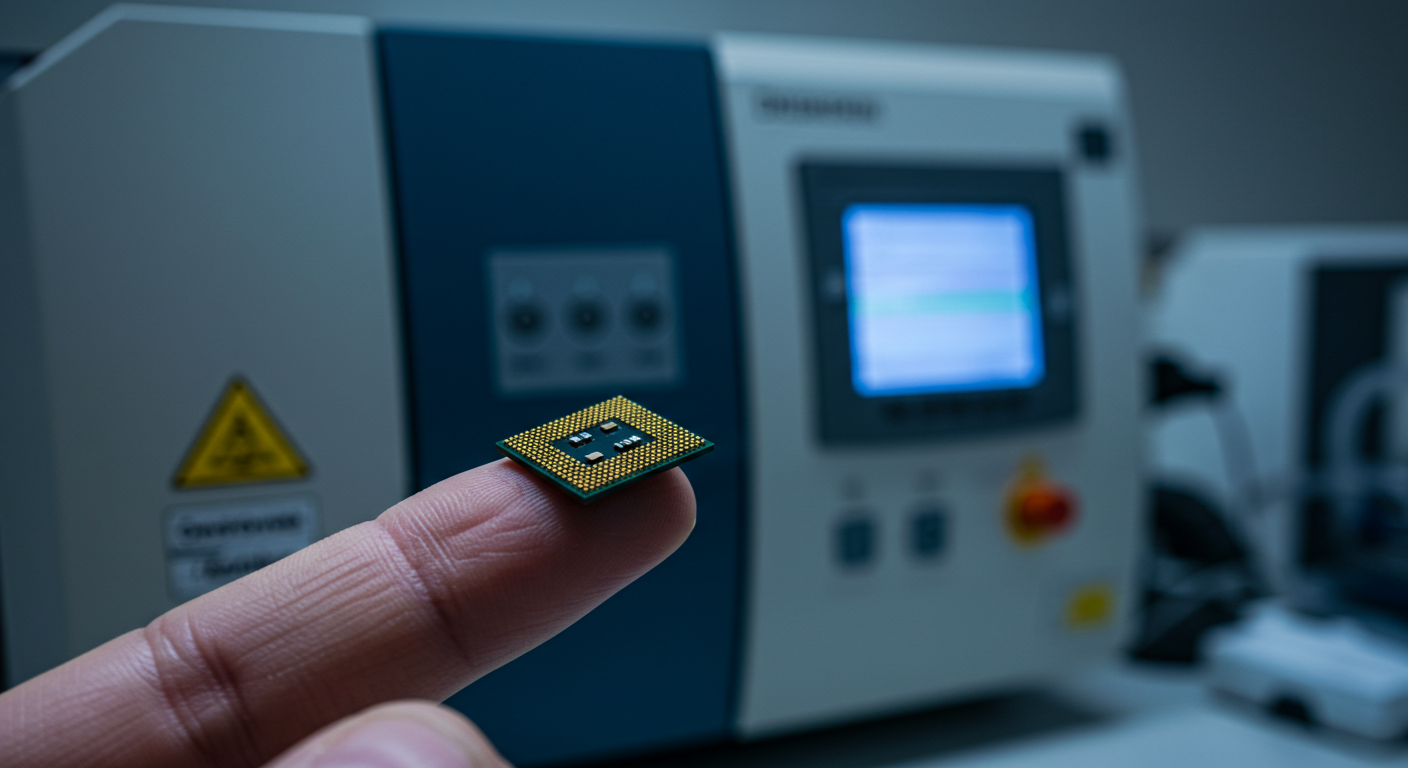
IBM did not unveil a sub-1-nanometer chip with 100 billion transistors on a single fingernail-sized die. What the company actually announced in May 2021 was what it called the world’s first 2-nanometer chip technology, demonstrated on a fingernail-sized test chip containing 50 billion transistors.
That distinction matters because semiconductor headlines often blur the line between a lab milestone, a future roadmap, and a product consumers can actually buy. IBM’s announcement was significant on its own terms, but the viral version overstates both the transistor count and the process node.
What IBM Actually Announced
IBM said its researchers had developed a 2nm chip technology intended to push semiconductor scaling beyond then-current designs. The company described the demonstration chip as roughly fingernail-sized and said it packed 50 billion transistors onto that surface.
There is no support in the source material for the claim that IBM unveiled a sub-1-nanometer chip, and the 100 billion transistor figure does not match IBM’s published description of the 2021 announcement. The supported headline is simpler: IBM unveiled a research demonstration of 2nm chip technology.
Why the Original Claim Is Misleading
The misleading version appears to combine separate ideas into one dramatic statement. In semiconductor coverage, research milestones are often mixed together with projections about future generations or broad comparisons across the industry.
That can create the impression that a company has already shipped a far more advanced product than it actually has. In this case, IBM’s documented result was a 2nm research breakthrough, not a sub-1nm launch, and the published transistor count was 50 billion, not 100 billion.
Separating verified figures from speculation is especially important in chip manufacturing, where node names can carry both technical and marketing meaning. A breakthrough can be real without matching every amplified claim that circulates online.
What Made IBM’s 2nm Chip Technology Significant
The real achievement was still substantial. IBM presented the 2nm result as a major step toward increasing transistor density and improving energy efficiency as traditional scaling becomes harder.
A key part of the advance was the use of nanosheet transistors, often described as a gate-all-around design. In simple terms, this structure gives engineers better control over electrical current as components shrink, helping reduce leakage and maintain performance at smaller scales.
That architectural shift is one reason the announcement drew attention beyond IBM itself. As Reuters and AnandTech noted at the time, it pointed to a practical path for continuing chip improvements even as older transistor approaches run up against tougher physical limits.
The Performance and Efficiency Claims
IBM said the 2nm technology could deliver about 45% higher performance at the same power level, or about 75% lower energy use at the same performance level, compared with 7nm chips. Those figures were presented as projections tied to the demonstrated technology.
They should not be read as guaranteed outcomes for every future laptop, phone, or server built on a similar process. Real-world results depend on manufacturing choices, chip design, software, thermals, and the economics of mass production.
Even so, the potential implications were easy to see. Better efficiency can extend battery life in mobile devices, reduce electricity use in data centers, and help support increasingly demanding computing tasks such as AI and high-performance processing.
Research Demo vs. Product You Can Buy
Another important point is that IBM’s announcement was about a demonstrated technology, not a retail chip launch. A successful lab prototype does not immediately become a mass-market processor.
Commercializing a new process usually takes years and depends on manufacturing partners, production yields, tooling, and whether the economics make sense at scale. That is why a genuine research breakthrough may take a long time to appear in shipping devices, if it appears in the same form at all.
So the announcement was not fake or trivial. It was simply at an earlier stage than many viral summaries implied.
What This Means for the Semiconductor Race
IBM’s 2021 announcement mattered because it showed that the industry still had credible ways to keep pushing transistor density and energy efficiency forward. It also underscored how much of the semiconductor race now depends on new transistor structures and manufacturing refinement, not just shrinking dimensions in a straightforward way.
It is also worth remembering that labels such as 2nm do not map perfectly across companies. Process-node branding has become partly a shorthand for relative progress rather than a direct apples-to-apples measurement.
The bottom line is that IBM did not unveil a sub-1-nanometer chip with 100 billion transistors. It unveiled a 2nm chip technology research milestone with 50 billion transistors on a fingernail-sized test chip. That corrected version is less sensational, but it is still an important chapter in the ongoing effort to build faster, more efficient semiconductors.