How Microchip Manufacturing Is Approaching Physical Limits
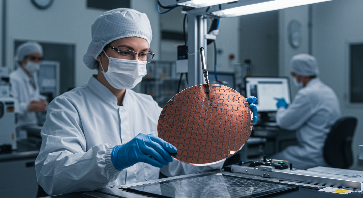
For decades, the semiconductor industry has relied on a simple formula for progress: make transistors smaller, pack more onto each chip, and deliver better performance. This approach, guided by Moore's Law, has powered everything from smartphones to supercomputers. But as manufacturing processes reach 2nm and approach sub-2nm scales, the industry is confronting a harsh reality—the fundamental laws of physics are starting to push back.
The End of Easy Scaling: Why Physics Is Catching Up to Moore's Law
Today's most advanced semiconductor foundries are producing chips with transistors just a few atoms wide. TSMC's 2nm process node, expected in production by 2025, will feature transistors with gate lengths approaching 12 nanometers—roughly 24 silicon atoms across. Intel's roadmap pushes even further, targeting what they call the "angstrom era" with sub-2nm processes.
This represents a dramatic shift from the engineering challenges that have historically defined chip manufacturing. For fifty years, Moore's Law held true largely because shrinking transistors was primarily a matter of improving manufacturing precision and materials engineering. The physics worked predictably: smaller transistors switched faster, consumed less power per operation, and allowed more functionality per chip.
But as transistors approach atomic dimensions, the reliable behavior that made this scaling possible begins to break down. What once were engineering problems requiring clever solutions have become fundamental physics barriers that may be insurmountable with current materials and architectures.
Quantum Effects and Atomic-Scale Challenges
At sub-5nm dimensions, quantum mechanical effects that were once negligible become dominant factors in chip design. Quantum tunneling, where electrons can "tunnel" through barriers that should block them classically, causes significant power leakage in modern transistors. This leakage can account for up to 40% of total power consumption in advanced processors, undermining the efficiency gains that smaller transistors were supposed to provide.
The behavior of electrons at these scales becomes increasingly unpredictable. In classical electronics, electrons flow through defined channels with predictable resistance and switching characteristics. At atomic scales, quantum effects introduce variability that makes each transistor behave slightly differently, complicating circuit design and reducing reliability.
Heat dissipation presents another critical challenge. As transistor density increases, the power density on chips approaches that of nuclear reactors. Current cooling solutions struggle to remove heat fast enough, leading to thermal throttling that limits performance. The situation worsens with quantum effects, as many quantum phenomena are temperature-sensitive and become more problematic as chips heat up during operation.
Perhaps most concerning are the reliability issues emerging from quantum mechanical interference. When millions of atomic-scale transistors operate in close proximity, quantum interference between neighboring devices can cause unexpected switching behavior and signal degradation that traditional error correction methods struggle to address.
Manufacturing Precision Hits the Light Barrier
Creating these impossibly small features requires extreme ultraviolet lithography, which uses light with a wavelength of 13.5 nanometers. However, the industry now faces a fundamental optical limit: trying to create features smaller than the wavelength of light used to pattern them.
Current 2nm processes already create features smaller than the EUV wavelength, requiring complex multi-patterning techniques where the same layer is exposed and etched multiple times to achieve the desired resolution. Each additional patterning step increases manufacturing complexity, reduces yield, and introduces new opportunities for defects.
The alignment precision required for these multi-patterning processes pushes current manufacturing equipment to its limits. Errors of even a single nanometer can cause circuit failures, yet maintaining this precision across 300mm wafers with billions of features remains an enormous challenge. As features continue shrinking, these alignment tolerances become even more demanding.
Beyond Silicon: Material Science Frontiers
Silicon, the foundation of the semiconductor industry for over half a century, faces fundamental limitations at atomic scales. Its electronic properties, which made it ideal for larger transistors, become problematic when channels are only a few atoms wide. Electrons can scatter unpredictably off surface atoms, reducing mobility and making transistor behavior less predictable.
Research into alternative materials has intensified, with III-V compound semiconductors like gallium arsenide showing promise for their superior electron mobility. These materials could potentially maintain better electrical characteristics at atomic scales, but they present significant manufacturing challenges.
Carbon nanotubes and graphene represent potentially revolutionary alternatives, offering exceptional electrical properties and atomic-scale precision. However, integrating these materials into mass manufacturing remains extremely challenging. Current techniques for growing and placing carbon nanotubes lack the precision and reliability required for commercial chip production.
The challenge isn't just finding better materials—it's integrating them with the hundreds of billions of dollars invested in silicon-based manufacturing infrastructure. Any new material must either work within existing fabrication processes or justify completely rebuilding the industry's manufacturing base.
Industry Pivot: 3D Architecture and Advanced Packaging
Faced with the limits of traditional 2D scaling, the industry is increasingly turning to vertical solutions. Modern memory chips already stack dozens of layers vertically, and logic processors are beginning to adopt similar approaches. This 3D integration allows continued increases in transistor density without requiring smaller individual transistors.
Through-silicon vias enable electrical connections between stacked layers, though they introduce new challenges in thermal management and manufacturing complexity. Each additional layer compounds heat dissipation problems, as internal layers become increasingly difficult to cool effectively.
Chiplet architectures represent another approach, breaking large monolithic processors into smaller, specialized chips that are packaged together. This allows manufacturers to optimize different parts of a system using different processes and materials, potentially improving yields and reducing costs. However, inter-chiplet communication introduces latency and power overhead that traditional on-chip connections don't face.
Advanced packaging technologies like 2.5D interposers and through-package vias enable tighter integration between multiple chips, but these solutions add significant complexity and cost to the manufacturing process.
Economic Reality: When Physics Meets Business
The economic pressures accompanying these physical limits are reshaping the entire industry. Leading-edge fabrication facilities now cost over $20 billion to construct, with each new generation requiring substantially higher investments. TSMC's most advanced fabs represent some of the most expensive manufacturing facilities ever built.
The return on these investments is diminishing as the performance benefits of each new process node become smaller. While moving from 28nm to 14nm provided substantial improvements in power and performance, the gains from 5nm to 3nm are more modest, even as development costs continue rising exponentially.
This economic reality is driving industry consolidation. Only a handful of companies—primarily TSMC, Samsung, and Intel—can afford to develop leading-edge processes. Many other semiconductor manufacturers are choosing to remain on older, more cost-effective nodes rather than chase the bleeding edge.
The concentration of advanced manufacturing capability in so few facilities creates supply chain vulnerabilities and pricing pressures that ripple throughout the technology industry. As leading-edge capacity becomes more constrained and expensive, the cost of cutting-edge processors continues rising.
The Path Forward: Redefining Progress in Chip Design
The industry's response to these challenges involves fundamentally redefining what progress means in semiconductor development. Rather than pursuing general-purpose performance improvements through smaller transistors, manufacturers are increasingly focusing on specialized processors optimized for specific workloads.
AI accelerators, graphics processors, and application-specific integrated circuits can achieve better performance per watt by optimizing their architecture for particular tasks rather than relying purely on transistor scaling. This specialization allows continued performance improvements even when general-purpose processors hit scaling limits.
Software-hardware co-design is becoming increasingly critical as hardware improvements become more incremental. Optimizing software to better utilize available hardware resources can provide performance gains that pure hardware scaling cannot match.
Breakthrough technologies like quantum computing, optical interconnects, and neuromorphic processors remain in development, but timeline estimates for commercial viability continue extending. Most experts believe practical quantum computers for general computing applications remain at least a decade away, while optical processing faces similar integration challenges as alternative semiconductor materials.
In this post-Moore's Law era, progress may be measured less by raw transistor counts and more by energy efficiency, specialized performance, and system-level optimization. The easy gains from shrinking transistors are ending, but the industry's capacity for innovation in architecture, materials, and manufacturing continues driving technological advancement forward.