How Microchip Manufacturing Is Approaching Physical Limits
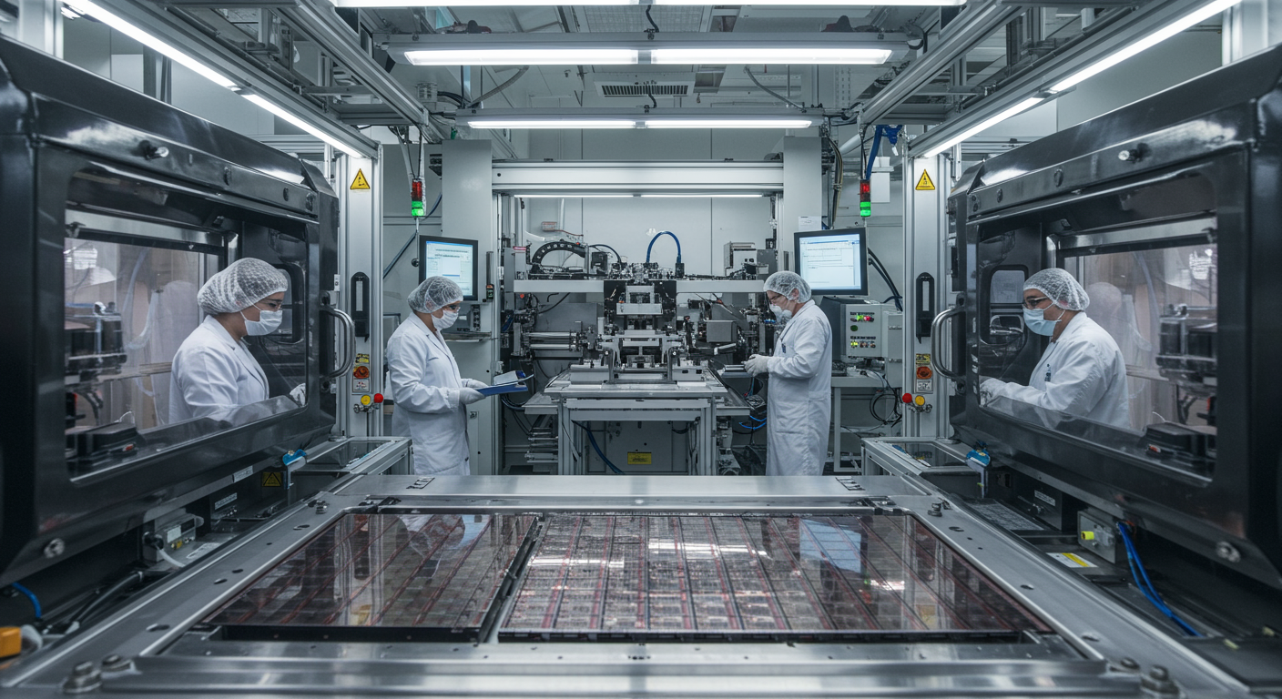
The relentless march of semiconductor technology toward smaller, faster, and more efficient microchips is encountering a formidable opponent: the laws of physics themselves. As the industry pushes manufacturing processes to 3nm and beyond, engineers are grappling with fundamental limits that threaten to end decades of predictable progress.
The Wall We're Hitting: Physical Limits at Atomic Scale
Today's cutting-edge semiconductor manufacturing processes are creating transistors that span just dozens of atoms in width. At these incredibly small scales, the classical behavior of electrons begins to break down, leading to quantum effects that were once theoretical concerns but are now practical engineering challenges.
Quantum tunneling has emerged as one of the most significant obstacles. When transistor barriers become thin enough—sometimes just a few atoms thick—electrons can spontaneously "leak" through what should be impermeable walls. This phenomenon causes increased power consumption and reduced reliability, undermining the very benefits that smaller transistors were supposed to provide.
Gate oxides, the insulating layers that control transistor switching, now measure only a few atoms in thickness. Engineers are approaching the point where these critical components cannot be made any thinner without losing their essential properties. Meanwhile, the concentration of transistors in modern processors generates heat densities that threaten to damage the delicate structures they're meant to protect.
Where Moore's Law Breaks Down
For decades, Moore's Law provided a reliable roadmap for the semiconductor industry, predicting that transistor density would double approximately every two years. However, this traditional scaling approach is no longer delivering proportional performance gains.
Power consumption has become a critical bottleneck. While transistors continue to shrink, their power efficiency improvements have slowed dramatically. In many cases, power consumption is actually increasing faster than performance improvements, creating a concerning trend for everything from smartphone batteries to data center operating costs.
Manufacturing defect rates are climbing as feature sizes approach atomic scales. The precision required to consistently create structures measuring just a few nanometers pushes manufacturing equipment to its limits, resulting in lower yields and higher costs. According to the Semiconductor Industry Association, the economic reality has become stark: the cost of building new fabrication facilities is doubling roughly every four years, making it increasingly difficult to justify the massive investments required.
Engineering Workarounds: Going Up Instead of Shrinking Down
Faced with the limitations of traditional scaling, the semiconductor industry is embracing vertical integration—literally. Three-dimensional chip architectures stack components vertically rather than spreading them across a single plane, allowing for greater functionality without requiring smaller feature sizes.
Chiplet designs represent another innovative approach, connecting specialized processors optimized for specific tasks rather than creating monolithic chips that attempt to do everything. This modular approach allows manufacturers to optimize different components using different processes, potentially achieving better overall performance than traditional designs.
Advanced packaging techniques are replacing the assumption that all components must be manufactured on a single piece of silicon. Through-silicon vias and other sophisticated interconnect technologies enable complex multi-chip assemblies that can outperform traditional single-chip solutions while being more economical to manufacture.
Beyond Silicon: The Materials Revolution
Silicon has been the foundation of the semiconductor industry for decades, but researchers are actively exploring alternative materials that could enable continued progress. III-V semiconductors, including compounds like gallium arsenide and indium gallium arsenide, offer superior electrical properties for certain applications, though they come with significant manufacturing challenges.
Two-dimensional materials such as graphene and transition metal dichalcogenides have captured significant research attention due to their unique electronic properties, according to research published in Nature's Electronic Materials and Devices journal. These materials can theoretically enable transistors with exceptional performance characteristics, though translating laboratory demonstrations into mass production remains a significant hurdle.
Carbon nanotube and nanowire transistor research continues to show promise, with some demonstrations achieving performance levels that exceed traditional silicon devices. However, the challenge lies not in proving these technologies work, but in manufacturing them reliably and economically at the scales required for commercial products.
Manufacturing at the Edge: EUV and What Comes Next
Extreme ultraviolet (EUV) lithography represents one of the semiconductor industry's most significant recent technological achievements. By using light with wavelengths far shorter than previous generation systems, EUV enables the precise patterning required for current cutting-edge processes.
High numerical aperture EUV systems are pushing resolution limits even further, though each improvement comes with exponentially increasing complexity and cost. The machines required for these processes are among the most sophisticated manufacturing tools ever created, with price tags exceeding $200 million per unit.
Alternative patterning techniques, including directed self-assembly, offer potential paths forward when traditional lithography reaches its limits. Atomic layer deposition and other precision manufacturing methods are enabling the creation of structures with atomic-level precision, though scaling these techniques to high-volume production remains challenging.
Rethinking Computing: Alternative Paradigms
As traditional semiconductor scaling approaches its limits, researchers are exploring fundamentally different approaches to computation. Neuromorphic computing attempts to mimic the architectures found in biological brains, potentially offering dramatic improvements in energy efficiency for certain types of problems.
Quantum computing represents perhaps the most radical departure from traditional approaches, using quantum mechanical effects to perform calculations that are impossible with classical computers. While quantum systems excel at specific types of problems, they are unlikely to replace traditional computers for most applications in the near term.
Optical computing, which uses photons instead of electrons to carry information, offers the potential for dramatically faster processing speeds and lower power consumption. However, the challenges of creating practical optical logic gates and memory systems have proven formidable.
The timeline for these emerging technologies varies significantly, notes MIT Technology Review's computing research. While some neuromorphic and quantum computing applications are entering practical use today, widespread adoption of alternative computing paradigms likely remains years or decades away.
The semiconductor industry stands at a crossroads. While the traditional path of making transistors smaller is approaching fundamental limits, the combination of architectural innovations, new materials, advanced manufacturing techniques, and alternative computing paradigms suggests that the age of computing progress is far from over. The solutions may look very different from the approaches that brought us to this point, but the underlying drive for better, faster, and more efficient computing continues to push the boundaries of what's possible.